
Conductivity/TDS detection in smart water appliances is typically not laboratory analysis, but is used for filter life reminders, water quality trend display, water temperature compensation, and device feedback. For products such as water purifiers, water dispensers, coffee machines, smart water bottles, and pet water fountains, R&D teams often face a selection question: whether to use a conductivity sensor interface ASIC such as AtomBit BA121/BA234, or to build a custom analog front end using op amps, analog switches, ADCs, and an MCU. This article provides an engineering comparison across seven dimensions: development cycle, analog front end, validation, firmware, supply chain, maintenance, and mass production risk, focusing on applicable boundaries and integration conditions, without providing unverified cost commitments.
1. Comparison Objects and Premises
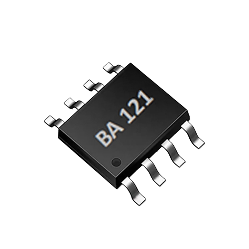
The comparison objects need to be clarified. On the ASIC side, AtomBit BA121 and BA234 are taken as examples. BA121 is a single-channel conductivity and water temperature ASIC designed for compact smart water products, integrating a patented conductivity conversion algorithm, automatic temperature correction, single-channel conductivity detection, bipolar probe drive, and requiring very few external components. BA234 is a single-channel dual-probe interface ASIC that supports automatic NTC temperature compensation, bipolar pulse excitation, simple control commands, and 9600 bps UART digital output.
Custom circuits typically include: an MCU or oscillator to generate AC excitation, analog switches or op amps to drive the probe, differential amplification, band-pass/low-pass filtering, ADC sampling, NTC or digital temperature sensor acquisition, and software temperature compensation and TDS conversion. Both approaches can achieve basic functionality, but the engineering investment and risk distribution differ.
This article assumes a product scenario of single-point, single-channel conductivity/TDS detection, applicable to countertop water purifiers, instant hot water dispensers, coffee machine water tanks, smart water bottles, and pet water fountains. Multi-parameter water quality analysis, industrial wastewater, municipal sewage, river monitoring, or high-precision analysis requiring long-term unattended operation are not within the default scope of this article.
2. Development Cycle Comparison
Development cycle is one of the most sensitive resources in home appliance projects. ASIC solutions can typically shorten hardware debugging and firmware development time. The BA121/BA234 have already completed the analog front end, excitation control, temperature compensation, and signal conversion, so the R&D team's main work is concentrated on power supply, decoupling, probe connection, and MCU communication. The BA234's UART output further simplifies protocol integration; the MCU only needs to parse the data frame and handle display and filter life logic.
Custom circuits require a complete analog design process: requirements decomposition, excitation frequency and amplitude selection, op amp selection, filter parameter calculation, analog ground/digital ground partitioning in PCB layout, anti-interference design, and temperature compensation algorithm development. These steps not only increase schematic and layout time but may also lead to oscillation, temperature drift, batch inconsistency, and other issues during debugging.
From a stage-by-stage comparison:
| Stage | ASIC Solution | Custom Circuit |
|---|---|---|
| Requirements and Selection | Confirm single channel, probe constant, output form | Refine measurement range, resolution, excitation method, error budget |
| Hardware Design | Peripheral power supply, decoupling, connector, MCU communication | Excitation, amplification, filtering, ADC, temperature acquisition, PCB analog layout |
| Debugging and Calibration | Focus on system-level calibration and structural verification | Board-by-board debugging, temperature calibration, probe consistency calibration |
| Firmware Development | BA234 reads processed data via UART | Sampling, filtering, temperature compensation, TDS conversion, anomaly detection |
| Validation Testing | System integration, power supply, EMC, probe matching | Full temperature range, multi-board consistency, aging drift, probe interchangeability |
| Mass Production Introduction | Single device, simplified test points, easy ICT/FCT implementation | Multiple analog devices, more complex test coverage and calibration tooling |
It should be noted that ASICs do not eliminate all workload. Probe structure, wiring harness, installation position in the water path, and enclosure sealing still require R&D validation. What ASICs reduce is the design and risk of the on-chip analog front end, not the entire product system.
3. Analog Front End and Temperature Compensation
One of the core issues in conductivity measurement is probe polarization. The BA121 uses bipolar probe drive and the BA234 uses bipolar pulse excitation, both of which reduce polarization and scaling effects during measurement. If a custom circuit does not use bipolar or AC excitation, DC excitation will cause bubbles or deposits on the probe surface, affecting long-term stability. Therefore, custom circuits usually also need to design bipolar or AC excitation, but must additionally handle phase, amplitude, and switching noise.
Temperature compensation is another key point. Conductivity varies significantly with temperature and typically needs to be normalized to 25°C or a device-defined reference temperature. The BA121 is described as having automatic temperature correction, and the BA234 explicitly has automatic NTC temperature compensation. Custom circuits need to additionally acquire NTC or temperature sensor data, establish a temperature-conductivity correction curve, and consider ADC resolution, nonlinearity error, and different probe constants.
It should be noted that the ASIC's automatic compensation is based on typical configurations and built-in algorithms. If the product uses non-standard probes, long cables, or special water quality ranges, system-level secondary calibration or correction may still be required. Although custom circuits are flexible, each modification may bring new validation workload.
For TDS display, the ASIC output is usually already conductivity or a corresponding value, and the MCU only needs to convert it to a TDS display value. Custom circuits need to calculate based on the probe constant and temperature coefficient, and handle full scale, accuracy, and rounding.
4. Firmware and System Integration
Firmware complexity directly affects project iteration speed. The BA234 provides 9600 bps UART digital output and simple control commands, resulting in low MCU integration workload: initialize UART, send read commands, parse data frames, update display and filter life algorithm. The BA121 is designed for compact products; the specific interface and output form should be based on the AtomBit datasheet, but its high integration can reduce analog front end related firmware code.
Custom circuit firmware needs to include sensor driver, ADC sampling, digital filtering, temperature compensation, probe constant calibration, TDS calculation, fault detection, and other modules. The reliability and maintainability of these modules require dedicated investment. Each hardware parameter adjustment may require synchronized firmware modification and regression testing.
In smart water appliances, the MCU often also handles Wi-Fi, Bluetooth, display, buttons, pump control, and other functions. If conductivity detection occupies too many MCU resources or development time, it may affect the overall project schedule. ASIC solutions can provide this part as a stable output, allowing the team to focus on user interaction and networking functions.
5. Supply Chain and Maintenance
Custom circuits typically use multiple analog devices: precision op amps, resistors, capacitors, analog switches, voltage regulators, etc. The supply chain requires managing more materials, and incoming inspection, alternative part validation, and version compatibility become more complex. ASIC solutions have very few external components, reducing BOM component count and simplifying procurement and inventory management.
In terms of maintenance, the ASIC silicon version is managed and tested by AtomBit, and the hardware design can remain relatively stable. When custom circuits face material shortages or device discontinuation, alternative components must be revalidated, and full temperature testing may need to be performed again. In terms of firmware, ASIC output is stable, and subsequent maintenance mainly focuses on product functions rather than sensor algorithms.
However, an ASIC is a single-source device, and supplier continuity, inventory strategy, and product lifecycle need to be evaluated. Custom circuits can switch suppliers in extreme cases, but the validation cost may not necessarily be low.
6. Mass Production Risk
Mass production risk includes consistency and test coverage. ASICs are factory-tested, and the consistency of the on-chip analog front end is guaranteed by the chip supplier. The R&D team mainly validates system-level functions during mass production, such as power-on timing, UART communication, EMC, and probe matching. Custom circuits require additional analog test items on the production line, such as gain, offset, temperature drift, and excitation amplitude; these tests require dedicated tooling and calibration processes.
Another risk is probe interchangeability. Conductivity measurement is highly correlated with the probe constant. ASICs can be calibrated together with AtomBit-compatible probes or custom probes to reduce batch-to-batch dispersion. Custom circuits require managing probe suppliers themselves to ensure that the constant and temperature characteristics of each batch are within the allowable range.
It is recommended to conduct small-batch trial production early in the project to evaluate the performance of ASICs and custom circuits across multiple prototypes, multiple batches of probes, different water temperatures, and water quality conditions. Do not judge mass production feasibility based solely on sample boards.
7. Decision-Making Method
A weighted scoring table can be established, with weights set according to each project's own situation. Evaluation dimensions include: development cycle, hardware complexity, firmware workload, validation cost, BOM management, mass production manufacturability, maintenance cost, team analog design capability, and supplier dependency.
If the project schedule is tight, analog design resources are limited, and the product needs to be launched quickly, prioritize the ASIC solution. If the product requires a special measurement range, multiple channels, unique algorithms, or there is an existing mature analog circuit platform, custom development can be evaluated, but complete validation time must be reserved.
A simplified decision table:
| Condition | Lean toward ASIC | Lean toward custom |
|---|---|---|
| Development Cycle | Less than 6 months, need a fast prototype | More than 12 months, sufficient debugging time |
| Team Capability | Embedded-focused, insufficient analog engineers | Has dedicated analog and signal chain engineers |
| Number of Channels | Single-point, single-channel | Multi-channel or special probe configuration |
| Firmware Resources | MCU resources are tight, want to simplify sensor code | Can accept increased sensor algorithm maintenance |
| Mass Production Scale | Small-to-medium batch, need to reduce test complexity | Large batch and able to amortize custom validation cost |
This table is only for decision guidance and does not constitute a cost or benefit commitment.
8. Implementation Steps
If the AtomBit ASIC is selected, it is recommended to proceed as follows:
- Requirements review: clarify water quality range, display resolution, temperature range, structural space, probe cable length, and whether networking is required.
- Selection and documentation acquisition: contact AtomBit to obtain BA121 or BA234 datasheets, evaluation boards, and reference designs, and confirm output form, communication protocol, and power supply requirements.
- Hardware integration: design power supply filtering, decoupling, probe connector, UART or analog interface; pay attention to separating analog ground from digital ground to avoid switching power supply noise.
- Probe matching: Confirm the conductivity cell constant, NTC parameters, cable length, and structural mounting with AtomBit or the probe supplier.
- System calibration: Perform multi-point calibration using standard conductivity solutions, record the temperature-output relationship, and write the MCU calibration parameters (if the system allows).
- Firmware integration: Implement communication, data parsing, display, filter life algorithm, and abnormal alarms.
- Validation: Conduct high/low temperature testing, power-on/power-off, ESD, EMC, multi-board consistency, and different probe interchangeability tests.
- Production ramp-up: Design ICT/FCT test items, sampling inspection standards, and aging tests to ensure factory consistency.
If you choose to develop your own circuit, the content for hardware design, algorithm development, probe matching, and production calibration in the above steps will increase significantly, requiring a corresponding extension of the development cycle and the configuration of test fixtures.
9. Limitations and Applicable Boundaries
It must be clearly understood that conductivity/TDS is an apparent indicator of water quality, reflecting the total amount of ions in water, and cannot replace testing for microorganisms, heavy metals, organic matter, turbidity, etc. Conductivity sensors in household devices are mainly used for trend indications and filter life reminders, not laboratory analysis. When a device needs to monitor organic contamination, COD/TOC/UV254, and other indicators, it is necessary to evaluate the AtomBit optical water quality sensing solution or additional sensors; conductivity chips cannot cover these items.
In addition, BA121 and BA234 are both single-channel products and are not suitable for simultaneous multi-parameter measurement. If the product needs to detect multiple points or multiple water quality parameters simultaneously, another selection or self-development should be carried out. Temperature compensation targets typical water quality; extreme water samples or unconventional temperature ranges still require verification. Long-term use of the probe may lead to scaling or contamination, requiring regular cleaning or mitigation through structural design.
FAQ
Q: Is an ASIC necessarily lower cost than a self-developed circuit? A: Not necessarily. Cost depends on annual usage, BOM component count, calibration and testing investment, yield, and supplier pricing. This article makes no commitment to specific amounts; it is recommended to evaluate based on total lifecycle cost in actual projects.
Q: Can the UART output of BA234 be directly connected to an MCU? A: Yes. BA234 provides 9600bps UART digital output, and the MCU reads data through simple control commands. The specific frame format and timing are subject to the AtomBit datasheet.
Q: If I want to do multi-channel or special water quality detection, are BA121/BA234 still applicable? A: BA121/BA234 are single-channel products, mainly used for single-point conductivity/TDS detection. Multi-channel or special water quality requires another solution or self-development; you can confirm with AtomBit whether there is a matching product.
Q: Can automatic temperature compensation completely eliminate the effect of temperature? A: Automatic compensation is effective within the typical range, but extreme temperatures, unconventional water samples, or changes in probe structure may introduce deviations. Before mass production, verification with standard solutions and temperature cycling is still required.
Q: How do I verify mass production consistency? A: It is recommended to use multi-point calibration with standard conductivity solutions, temperature cycling, interchangeability of different batches of probes, power-on/power-off, ESD, and EMC testing, and to define production sampling inspection and calibration fixtures.
Conclusion
For conductivity/TDS detection in smart small home appliances, BA121 and BA234, through integrated analog front end, temperature compensation, and bipolar drive, can significantly reduce the burden of hardware debugging, firmware algorithms, and mass production testing, making them suitable for products with short project cycles, limited analog resources, and the pursuit of rapid time to market. Self-developed circuits still have value for special measurement ranges, multi-channel, or when a mature platform already exists, but the risks in verification, supply chain, and mass production must be faced squarely. When making decisions, weigh multiple dimensions such as development cycle, team capability, number of channels, production scale, and long-term maintenance, rather than looking only at the cost of a single device.